Raspberry Pi Pico PIO without the SDK
posted 2022 January 30
2646 words // est. 14 min. read
tags: embedded, programming
Currently, I am working on using the Raspberry Pi Pico to do some signal processing on instrument audio signals in real time. While the Pico has a 12-bit analog-digital converter (ADC) which I use to obtain samples, it lacks a digital-analog converter (DAC) which I would use to output processed samples. However, the MCU boasts what Raspberry Pi calls programmable I/O blocks (PIO) that a programmer can use to implement a wide variety of protocols like UART and I²C. Definitely within reach is the simple, one-way I²S protocol, a common protocol for transmitting audio samples to a DAC.
And so, I decided to implement I²S on top of a PIO state machine and use an external DAC to create the corresponding analog signal. Since I am writing the software on top of "bare metal" without the SDK, the RP2040 datasheet and I became fast friends. Along the way, I encountered a couple of bumps while referring to the datasheet and thought them useful to put together in more palatable words.
DSP on the RP2040?
There is more powerful silicon out there to achieve this, but I was intrigued by this new microcontroller from Raspberry Pi and wanted to see what it could handle. It is a relatively simple ARM Cortex M0+, but it also packs two cores, is simple, cheap, and widely available. I will be taking advantage of the dual core architecture to split the workload of the controller into two halves. One core will handle the signal processing, and the other will run the Tock embedded OS. I am augmenting Tock OS to control the signal processing core through the FIFO the cores share. Signal processing itself is not highly relevant to this post. I mainly focus on the quirks of creating an I²S-compatible peripheral out of the RP2040's programmable IO state machines. Without the SDK.
Without the SDK!?
Figuring out how one should write software to interact with hardware (given the hardware's capabilities and quirks) is a big part of the fun of working with embedded systems. Designing sensible, flexible software interfaces that intermediate interactions with hardware is a skill I try to hone regularly. This means doing more than writing functions to perform rote register reads and writes; it is an attempt at striking a balance between being efficient (code size, performance) and exposing an interface that will not let a developer mess up too easily. In this context I want to get to know how RP2040 works without any conveniences.
Additionally, my aforementioned personal project is based on the Tock embedded operating system. Tock is written in Rust, while the Pico SDK is written in C and C++. I enjoy programming in C and C++, and I enjoy programming in Rust, but I do not fancy putting them together, however feasible that may be.
One more thing... I have no desire to write an assembler.
One external resource I am leveraging is pio_proc from the
pio-rs
project.
This library will perform the translation from PIO assembly to opcodes at compile-time through Rust macro machinery.
Relying on this library to generate PIO assembly's corresponding binary representation is a convenience I will accept since it does not impede me learning how the RP2040's PIO hardware works.
No NIH syndrome in this respect.
First steps
To get started I dug through the basics of PIO in chapter 3 of the SDK documentation and authored code to configure the PIO blocks. Then I read an overview of the I²S protocol (Wikipedia has a nice graphic of the protocol) and came up with the following PIO:
    .wrap_target                      ; Loop back here upon reaching .wrap
left_ch:
    set pins, 0 side 0b00             ; Output the don't-care bit. Clock low.
    set x, 15 side 0b01               ; Set up counter. Cue on BCLK.
left_ch_loop:
    out pins, 1 side 0b00             ; Write the left channel bit.
    jmp x-- left_ch_loop side 0b01    ; Repeat to output 16 bits. Cue on BCLK.

right_ch:
    set pins, 0 side 0b10             ; Output the don't-care bit. Clock low.
    set x, 15 side 0b11               ; Set up counter. Cue on BCLK.
right_ch_loop:
    set pins, 1 side 0b10             ; Write empty right channel.
    jmp x--, right_ch_loop side 0b11  ; Repeat to output 16 bits. Cue on BCLK.
    .wrap                             ; Go to .wrap_target (line 1).
A mere eight instructions (highlighted above) out of the 32 we can fit in instruction memory. I am relying on the PIO to clock out the don't-care bit that heads off each sample transmission instead of supplying it in the incoming data stream. This made the PIO assembly a couple of instructions longer than it had to be.
A small PIO brief
I suspect that if you have dealt with any assembly, you will understand the structure of PIO easily. But if you've never seen PIO before, some elements may be hard to grasp without reading the documentation. For a brief explanation of a few concepts here...
SET and OUT instructions are two distinct ways to move values to locations.
SET takes a destination and a value and places the value at the destination
(set <destination> <value>).
x is a scratch register I use for looping in this case.
OUT takes a destination and a count of bits to move from its "pending output bit queue",
called the output shift register, or OSR,
to the destination
(out <destination> <bit count>).
The OSR itself receives data from the state machine's transmit FIFO
which accepts data from within the microcontroller destined to leave the system.
(in summary, inside μC → PIO TX FIFO → OSR → pin).
Side set is a handy capability that allows you to treat changing pin states as something that happens as a side-effect,
without itself taking up an instruction (gotta save on that instruction memory!).
Side sets are expressed with the additional side keyword and the new desired logic state.
The PIO above expresses the pin state as binary.
The side set is simultaneous with the instruction.
I am using side-sets to create the I²S bit and word clocks.
Wrapping happens at configurable instruction locations.
This is configurable on a per-state machine basis
(which I use in a bit).
The keywords .wrap and .wrap_target are not instructions but rather helpful hints to the assembler that allow it to automatically generate the corresponding indices to be written to the registers.
Initial PIO state
I wrote the encoded PIO assembly to instruction memory, configured the clock source, started piping some sample data to the PIO, excitedly hooked up my oscilloscope and got... nothing. No pins toggling.
Eventually, I noticed that the initial I/O direction for PIO pins is input, not output.
So that means all I had to do was prepend the set pindirs, 1 instruction to my assembly to use a pin as an output.
    set pindirs, 1

    .wrap_target
left_ch:
    set pins, 0 side 0b00
    ...
That is true, but... not all examples in the documentation head off the program with this instruction. So how do the examples achieve output without taking up precious instruction memory?
After some code-reading in the SDK, I noticed a bit of code doing something that neither the datasheet nor the SDK documentation go into detail about:
setting the I/O direction of pins prior to running the state machine by writing to the PIO block's INSTR register to forcefully execute an instruction.
In fact, force-executing PIO assembly is a common operation in the SDK PIO code.
The usage of most interest in this context is in the pio_sm_set_pindirs_with_mask function
(modified and annotated for presentation):
// Temporarily save away PIO pin configuration.
uint32_t pinctrl_saved = pio->sm[sm].pinctrl;
while (pin_mask) {
    uint base = (uint)__builtin_ctz(pin_mask);
    pio->sm[sm].pinctrl =
            (1u << PIO_SM0_PINCTRL_SET_COUNT_LSB) |
            (base << PIO_SM0_PINCTRL_SET_BASE_LSB);
    // Force-exec a SET PINDIRS to configure each pin's initial I/O direction.
    pio_sm_exec(pio, sm, pio_encode_set(pio_pindirs, (pindirs >> base) & 0x1u));
    pin_mask &= pin_mask - 1;
}
// Restore the state machine's PINCTRL configuration.
pio->sm[sm].pinctrl = pinctrl_saved;
While the INSTR register is documented as all other registers
and the datasheet covers forced instructions,
the datasheet's helpful topics never cover this trick
even though they go through great lengths to show readers other ways to write small, performant PIO assembly.
Essentially, this becomes a tradeoff between PIO instruction memory and code size.
Doing this saves PIO instruction memory, but adds growth to the code required to configure the PIO in this manner.
This is plenty worthwhile seeing as there is an abundance of flash on the RP2040 when you compare it to the miniscule 64 bytes of state machine instruction memory.
So we build up the instruction's binary representation and write the instruction during configuration:
let set_pindirs_instr =
    ENC_INSTR_SET
    // Target for the SET is PINDIRS who's value changes I/O direction.
    | 0b000_00000_100_00000
    // Caller-provided mask; 0 = input, 1 = output.
    // E.g., 0b010 means the first and third pins are inputs, second is output.
    | params.initial_pindir as u16;

// Force-execute the instruction.
self.registers.sm_ctrl[sm_no].instr.set(set_pindirs_instr as u32);
Note that we also must do this for side-set pins. The only difference being that we set the PIO base set pin to the first side-set pin before we do the above. Then we set the real set base pin value that the PIO machine should use during execution.
It works!
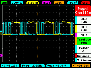
And with this, I was able to generate the below valid I²S signal! The yellow line is the word clock for indicating the left and right channel. The blue line is the sample data as a signed binary value. I have data for only one channel, so I opted to use the left (word clock low) channel and not the right channel.
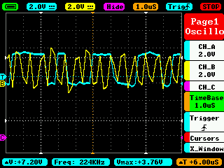
In the below screenshot, we start to see the limits of this oscilloscope. It is a pretty handy tool to have on hand, but it may be time to upgrade... The I²S bit clock runs 34 times faster than the word clock to clock out 17 bits for each channel. Recall that the first bit in an I²S word is a don't-care bit and I am using 16 bits per sample. In blue is the data, and in yellow is the bit clock. Notice even the data line trace is showing jaggedness. Still, we can just barely make out that the data signal is latched by the peripheral on the other end and the data changes only on a falling edge, just as the PIO assembly dictates.
Bigger step
I got this rigged up on a few breadboards and used a UDA1334ATS from NXP Semiconductors conveniently packaged on a breakout board by Adafruit to get the corresponding analog signal from the I²S data. It worked great! However... unfortunately, the UDA1334ATS has been EoL'ed since 2019. Not a good choice to use for the next few years. I needed to find another IC that would accept I²S and produce the corresponding analog signal. So I chose the PCM1771 and PCM1773 from Texas Instruments. The difference between the two is not relevant to this article, but their difference from the EoL'ed UDA1334ATS is relevant: the PCM177x requires an additional clock from the microcontroller for its own internal circuitry. This additional clock input, termed SCKI (for serial clock input), must run at either 128, 192, 256, or 384 times the sampling frequency! That means we now must provide:
- the bit clock,
- the word clock,
- the serial clock,
- and the sample data.
That's a lot of clocks.
So, it's back to the PIO assembly.
This time, however, there is a small twist preventing us from simply adding an additional side-set pin:
I cannot represent such an exceedingly fast clock signal within my current assembly.
Only small delays are possible,
and besides,
who would want to balloon the assembly for delays and nops after cranking up the PIO to run 128 × 44,100?
A more elegant solution is to just use another PIO state machine to generate SCKI.
The Pico has two PIO blocks that contain four state machines each. While each machine in a block functions separately from the other three, they all execute from the same 32 instructions-long memory. In order to run the two state machines separately, I have to be able to modify their wrapping points and their entry points.
Modifying the wrapping point
While it is easy to specify a single end and beginning wrapping point of a PIO program,
it is not so easy to specify them for two programs bundled into one.
For starters, I could no longer use the .wrap_target and .wrap directives,
even though pio_proc is useful and offers convenient access through a field on the struct if you define them in your code.
I do not have a better solution for this other than manually counting the instructions to find the values that will provide the desired wrapping behavior. But it may not need another solution, as this will work fine for any PIO program. No PIO program exceeds 32 instructions in length, so counting by hand is not too onerous a task.
So while I can do the following for one PIO state machine:
// Generate the PIO program for the following code at compile-time.
let i2s_pio = pio_proc::pio!(32, "
.wrap_target     ;; Come here from .wrap
  nop            ;; Do nothing
.wrap            ;; Go back to .wrap_target
");

let i2s_pio_config = pio::Parameters {
  // Obtain the wrapping source from the generated i2s_pio object.
  wrap_top: i2s_pio.wrap.source,
  // Obtain the wrapping target from the generated i2s_pio object.
  wrap_bottom: i2s_pio.wrap.target,
  ..pio::Parameters::default()
}
I cannot do it for a second (or third or fourth).
Modifying the entry point
Using a new entry point actually is in the datasheet as an example. This is possible by force-exec'ing an unconditional JMP to the index of the desired instruction.
let jmp_initial_instr =
    ENC_INSTR_JMP
    | params.entry as u16;
self.registers.sm_ctrl[sm_no].instr.set(jmp_initial_instr as u32);
The above snippet should look familiar.
It works just like the force-exec'ed SET to set pin I/O direction.
I also exposed a configuration option to change the entry point on a per-state machine basis.
PCM177x-compatible PIO
With those two capabilities added in my code, I was ready to update the PIO and run with it. And now, without further prolonging, here are the new PCM177x-compatible PIO programs:
    ;; bit 0 = BCLK, bit 1 = LRCLK
    .side_set 2

;;; I²S hardware logic (instructions 0 to 7)
left_ch:
    set pins, 0 side 0b00               ; Output DC bit. Clock low.
    set x, 15 side 0b01                 ; Set up counter. Cue on BCLK.
left_ch_loop:
    out pins, 1 side 0b00               ; Write the left channel bit.
    jmp x-- left_ch_loop side 0b01      ; Repeat to output 16 bits. Cue on BCLK.
right_ch:
    set pins, 0 side 0b10               ; Output DC bit. Clock low.
    set x, 15 side 0b11                 ; Set up counter. Cue on BCLK.
right_ch_loop:
    set pins, 1 side 0b10               ; Write empty right channel.
    jmp x--, right_ch_loop side 0b11    ; Repeat to output 16 bits. Cue on BCLK.

;;; PCM177x SCKI (instructions 8 to 9)
;;;
;;; Configuration:
;;; Assign a set pin for the clock output signal.
scki_loop:
    set pins, 0 side 0b00               ; Output clock high signal.
    set pins, 1 side 0b00               ; Output clock low signal.
Once I wrote the clock divider math, the PIO did its duty. I plucked a note on my violin. I obtained the corresponding output from the PCM1771.
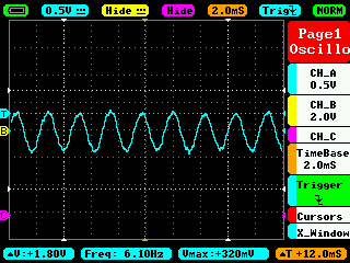
If I had minded enough, I would have brought the edge threshold down enough so that it would correctly report the signal frequency. If you do the math, you would be able to see that this is, in fact the result of me plucking the A string. The spacing between each vertical grey line is equivalent to 2 milliseconds, so the period of the waveform is 2ms and some change. If you fudge the number a bit to 2-point-something, like 2.2, this comes close to 440Hz. Do note, however, that I am sure my violin was out of tune during this testing...
Space-optimized PIO
Down to ten instructions is certainly "good enough". The later iteration of the PIO fits in instruction memory, is readable, well-commented, and it works. But let's think a little further about space optimization if we were squeezed for space.
We could eliminate the need for the separate, readable SCKI PIO assembly by having the second PIO state machine loop over two consecutive instructions from the first's PIO. The only code change we need is to delete the last two instructions. However, the configuration for the SCKI state machine changes:
let scki_pio_config = rp2040::pio::Parameters {
  // Use a side-set pin.
  side_set_count: 1,
  // Pin 14 will be a side-set pin.
  side_set_base_pin: 14,
  // Bottom of the execution wrap.
  wrap_top: 1,
  // Top of the execution wrap.
  // The naming seems kind of backwards,
  // but this is consistent with datasheet's convention.
  wrap_bottom: 0,
  ..rp2040::pio::Parameters::default()
}
- Use a single side-set pin.
- Configure that side-set pin's number.
- Set the wrapping point such that it will repeatedly execute any two consecutive instructions in the first's PIO. This means the SCKI PIO no longer has to specify a different entry point.
This should work (I have not tested this) since the I²S state machine outputs the bit clock that toggles between high and low using side sets. But, for readability's sake, I think the ten-instruction variant is fine.
Wrap-up
It is great that it fits in a mere ten instructions, but this does have its quirks:
- I have to manually count instructions to get the wrapping indices for each state machine. This is not too big of an issue, though, since PIO programs are limited to 32 instructions.
pio_procdoes not like seeing inconsistent side-set operations. Indeed, the library is only intended to translate valid PIO programs, and not specifying the side set when the directive indicates that side-sets should happen is invalid.
As an aside, I have made significant progress with this project. I have even gotten a decent audio signal to my instrument amp at this point and am working on cleaning up the wiring so I can prototype a board. That, however, I will leave to a future write-up at which point it will be in a more complete state. Back to the Pico...